- TOP
- Headlines Top Page
- Education
- New Manufacturing Process for SiC Semiconductor Wafers Being Developed by KGU and Toyota Tsusho

News and Topics
New Manufacturing Process for SiC Semiconductor Wafers Being Developed by KGU and Toyota Tsusho
2019.12.11
Currently, it is commonplace to use silicon (Si) wafers as substrate material for semiconductors. However, electrical loss occurs due to the properties of Si. SiC is a next-generation energy-saving material which can significantly reduce such loss. SiC has three times the bandgap*1 of Si, four times its thermal conductivity*2, and nine times its dielectric breakdown field strength*3. With such properties, SiC wafers allow for optimal electricity use and the miniaturization of cooling devices. The application of SiC wafers has begun in a wide range of fields, including the automotive industry, rail transport, home appliances, and electricity. Among these, there is high demand for the use of SiC wafers in electric vehicles such as EVs and HEVs, where there are high expectations placed on them.
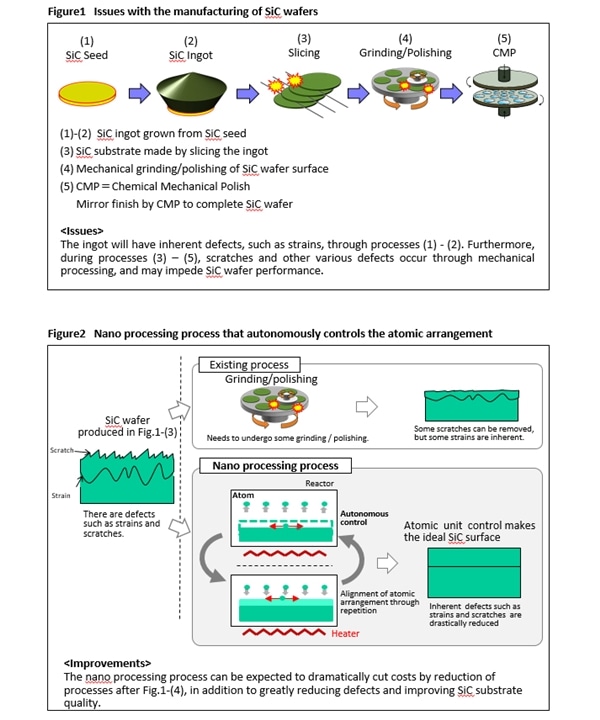
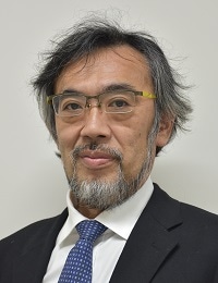
Compared to Si, the high-performance SiC wafer has issues in terms of quality and manufacturing cost. In the first place, there are many imperfections, such as defects and strains, in SiC ingots. Furthermore, in conventional manufacturing processes, the subsurface damages produced when mechanical processing is carried out on the SiC surface, such as scratches and other defects, may impede SiC performance. In addition, conventional mechanical processing requires multiple grinding and polishing processes, with little progress in cost reduction, which hinders SiC wafers from becoming widely used.
Kwansei Gakuin University is putting an emphasis on promoting the Green Mobility Materials and Manufacturing Technology Project (leader: Professor Tadaaki Kaneko, School of Science and Technology), which develops and is in possession of nano processing technology that autonomously controls the arrangement of surface atoms for contactless planarization of SiC wafers by means of thermal etching and growth (refer to Figure 2). To solve the issues of SiC wafers, Toyota Tsusho and Kwansei Gakuin University are working to establish technology for the nano processing of SiC wafers at the practical application level, and to develop manufacturing processes for mass production. Toyota Tsusho is aiming to popularize high-quality SiC wafers in various industries, such as the automotive field. In order to build a platform for introducing nano processing technology into the market, in cooperation with Kwansei Gakuin University, Toyota Tsusho will provide experts and information, in addition to carrying out intellectual property management and marketing.
*1 Bandgap: An index that shows resistance to high temperatures, with higher values showing better suitability for high-temperature operations. *2 Thermal conductivity: An index that shows the ability to release heat, with higher values showing better ease of cooling devices. *3 Dielectric breakdown field strength: This is the threshold value before matter breaks down when electrical voltage is applied. The larger this value, the harder it is for matter to break down, allowing products to be made smaller.